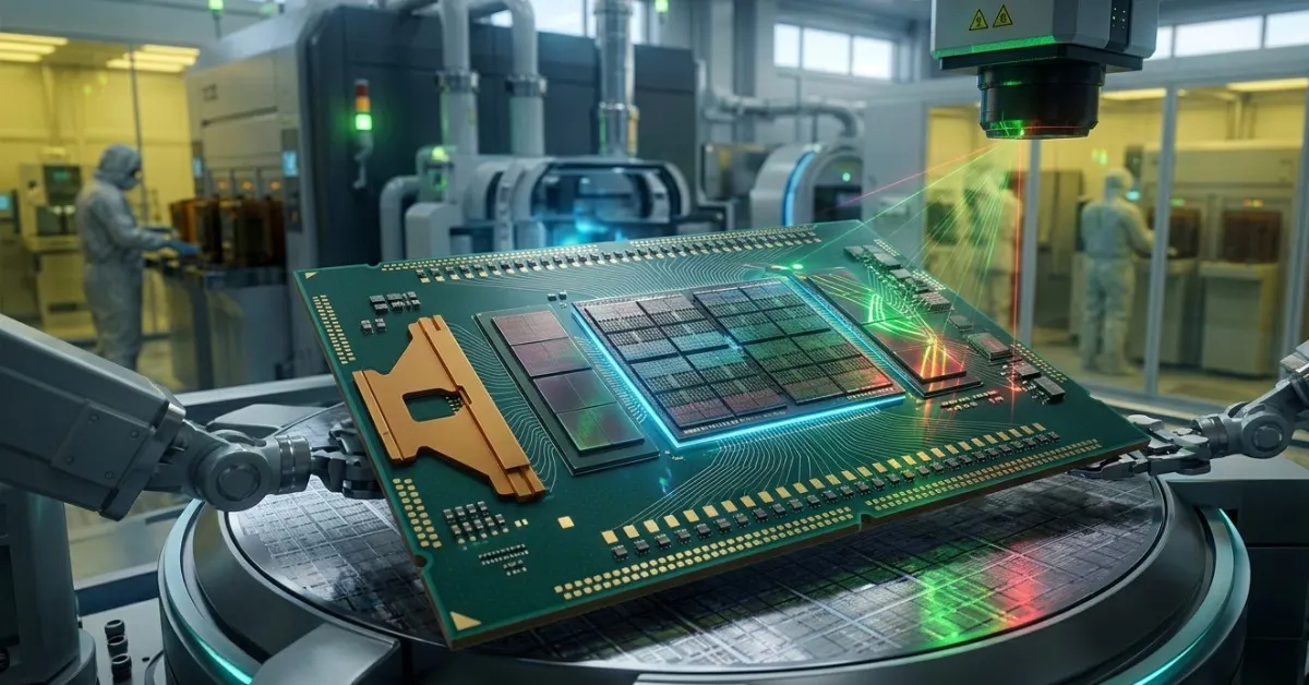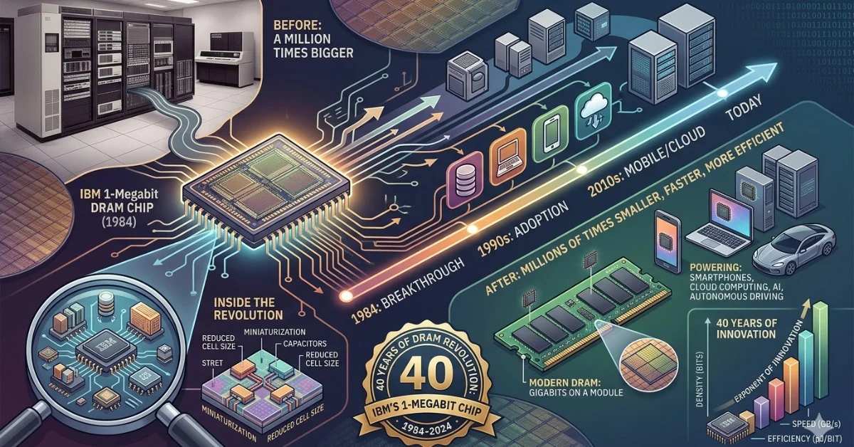
Forty years after IBM brought 1-megabit DRAM into commercial mainframe use, the milestone still explains why memory density matters. The chip itself looks modest by modern standards. One megabit is only 128 kilobytes. But in 1986, the move represented a major jump from the 64-kilobit and 256-kilobit parts that defined much of the earlier DRAM market. It helped mark the start of the megabit memory era.
The Computer History Museum records April 18, 1986, as the day newspapers reported IBM had become the first computer manufacturer to use a megabit chip in a commercial product, the IBM 3090. The Los Angeles Times archive described IBM as the first to begin volume production of the 1-megabit memory chip and the first to put it into mainframe computers. That point matters: the achievement was not only a lab demonstration, but a step into production systems.
Why the 3090 mattered
The IBM 3090 was a high-end mainframe line aimed at customers that needed large, fast and reliable computing systems. Adding denser memory helped IBM improve capacity without simply multiplying boards and physical components. In large systems, denser memory can reduce space, simplify design and support larger workloads. The 1-megabit chip therefore mattered because it connected semiconductor progress to real machines, not just technical papers.
IBM's own history of DRAM places the 1-megabit generation within a longer story that began with Robert Dennard's invention of DRAM in the 1960s. DRAM replaced older memory approaches because it could store data more cheaply and densely. Each density jump then changed what computer designers could build. The 1-megabit generation was one of those jumps.
The market story was more complicated
IBM's announcement was also read through the industrial rivalry of the 1980s. U.S. computer makers wanted proof that they could still lead in semiconductor manufacturing, while Japanese companies such as Fujitsu, NEC, Hitachi and Toshiba were pushing aggressively in memory. The milestone gave IBM a symbolic win, but it did not end Japan's strength in DRAM. Fujitsu, for example, had already developed a 1-Mbit DRAM in 1985 and later documented that technology as part of its semiconductor history.
That nuance is important. IBM's 1-megabit DRAM did not single-handedly decide the memory market. It showed that high-density DRAM had crossed from ambition to commercial use, and it helped push the rest of the industry toward megabit-class parts. The broader effect came later, as memory modules, PCs, workstations and peripherals adopted denser DRAM through the late 1980s and 1990s.
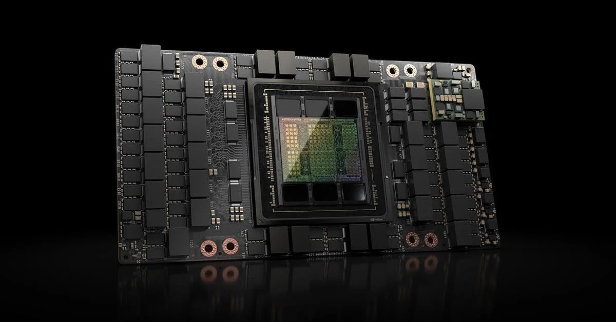
Today, the industry is talking about HBM, DDR5, DDR6 and memory shortages driven by AI data centers. The numbers are almost unrecognizable compared with 1986. Still, the lesson is familiar: every major jump in memory density changes what computers can do. IBM's 1-megabit DRAM was one of the steps that made modern memory scaling feel inevitable.