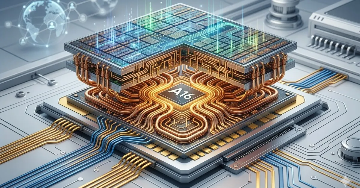
TSMC’s A16 process is moving into focus in 2026 because it is the company’s next major logic technology after N2 and N2P, with planned production in 2026. The important correction is timing: TSMC first debuted A16 at its North America Technology Symposium in April 2024, not as a brand-new April 2026 announcement. What matters now is that the node is approaching its intended production window, and its biggest architectural change is backside power delivery through TSMC’s Super Power Rail design.
Why backside power matters
A16 combines nanosheet transistors with Super Power Rail, a backside power delivery approach that moves power routing away from the front side of the chip. In conventional designs, signal lines and power lines compete for routing resources in the same crowded layers. By moving power delivery to the back side, TSMC can dedicate more front-side routing to signals while reducing resistance and improving power distribution.
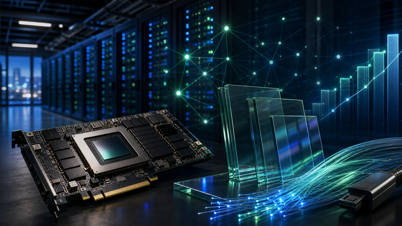
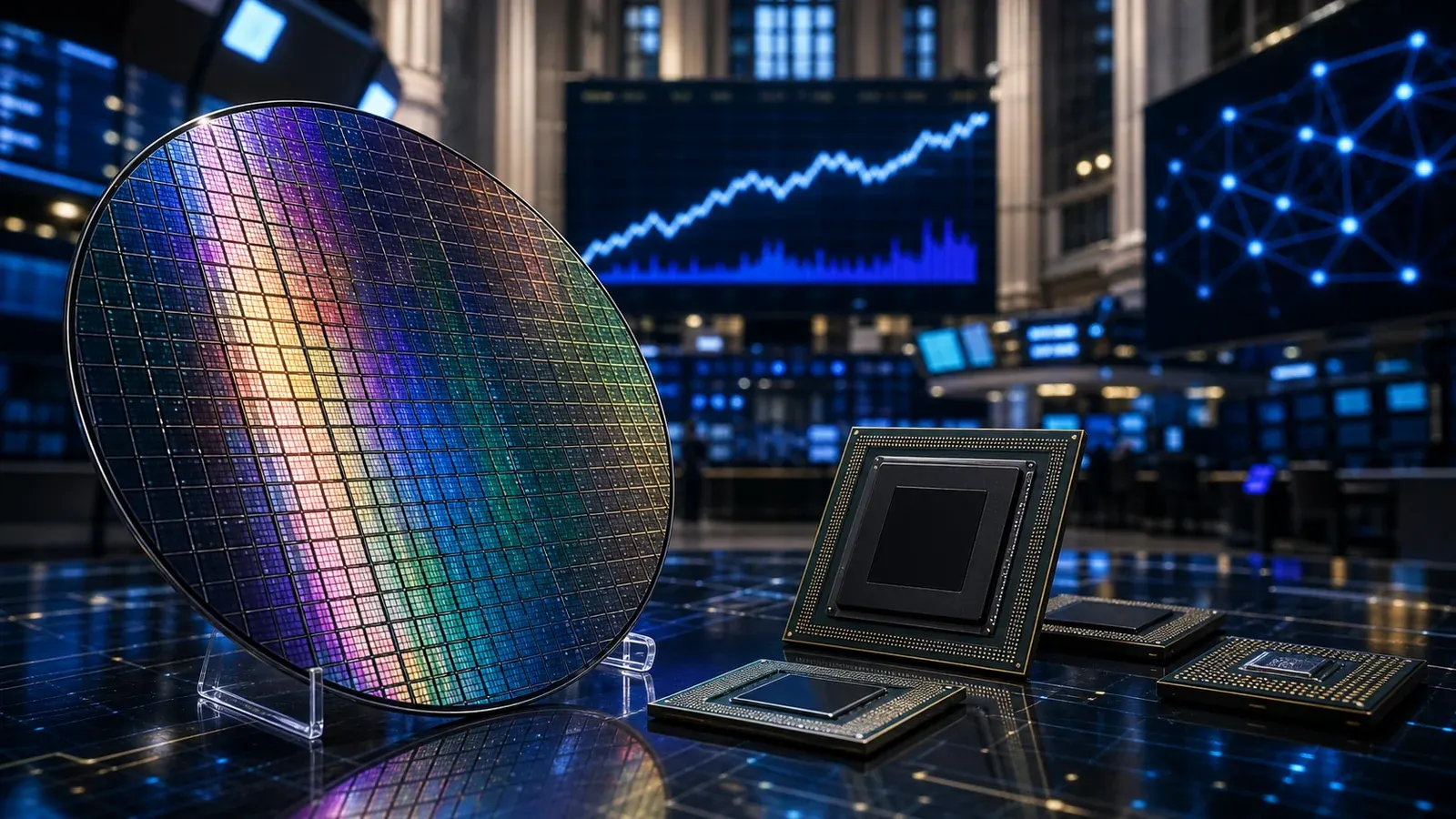
That change is especially relevant for high-performance computing chips, where dense power networks and complex signal routes are a constant design challenge. TSMC says A16 is designed for products such as data center processors and AI accelerators that need both higher performance and better power efficiency. The company’s public A16 page describes the node as combining advanced nanosheet devices with Super Power Rail to improve logic density and performance.
The official performance claims
Compared with TSMC’s N2P process, the company says A16 can deliver an 8% to 10% speed improvement at the same voltage, a 15% to 20% power reduction at the same speed and up to 1.10x chip density improvement for data center products. These are TSMC-provided figures, so they should be treated as foundry guidance rather than independent benchmarks. The numbers are still useful because they show how TSMC wants customers to think about A16: not only as a smaller node, but as a routing and power-delivery shift.
The node also sits inside a wider roadmap. TSMC said N2 was on track for production in the second half of 2025, while A16 would follow as the next technology on the roadmap. That sequence matters for chip designers deciding whether to target N2, N2P or A16. The more aggressive the design, the more likely it is to benefit from backside power delivery, but the more work it may require in design adaptation and validation.
AI, mobile and the production test
TSMC frames A16 around AI and high-performance computing, but the logic also applies to advanced mobile processors where efficiency per watt remains critical. The practical question is not whether backside power delivery is promising; it is how quickly customers can build designs around it and how reliably TSMC can manufacture those designs at scale.
That is why the next phase is less about naming and more about execution. If A16 delivers the promised speed, power and density gains in production silicon, it could mark an important shift in how leading-edge chips improve after conventional scaling becomes harder. If yields, design cost or early availability create friction, adoption may be slower and concentrated first in expensive data center chips.
For now, A16 is best understood as a 2026 production technology built around backside power delivery, not a surprise new node announced in 2026. The story to watch is whether TSMC can turn the Super Power Rail architecture from a roadmap milestone into reliable volume manufacturing for the next generation of AI and HPC chips.